Final Cut Pro的問題,透過圖書和論文來找解法和答案更準確安心。 我們找到下列懶人包和總整理
Final Cut Pro的問題,我們搜遍了碩博士論文和台灣出版的書籍,推薦蘋果梗寫的 Final Cut Pro職人剪片全攻略:一台 Mac 包辦影音剪輯、素材處理、調色技巧,打造流暢的高質感影片! 和Nahmani, David的 Logic Pro X - Apple Pro Training Series都 可以從中找到所需的評價。
另外網站Final Cut Pro vs Adobe: Which one is better? - Gitnux Blog也說明:Final Cut Pro is a professional video editing software application developed by Apple Inc. for the Mac platform. It allows users to edit, ...
這兩本書分別來自博碩 和所出版 。
臺北醫學大學 保健營養學系博士班 黃士懿、陳揚卿所指導 NGAN THI KIM NGUYEN的 Precision nutrition for children with early puberty: leveraging nutrigenomics and lipidomics analysis (2021),提出Final Cut Pro關鍵因素是什麼,來自於precocious puberty、central precocious puberty、systematic review、meta-analysis、gene-nutrient interaction、lipidomic analysis、LS/MS、biomarkers。
而第二篇論文長庚大學 奈米工程及設計碩士學位學程 周煌程、杨杰圣所指導 梁文顏的 低功耗高性能電流式感測放大器設計 (2020),提出因為有 電流式電路、感測放大器的重點而找出了 Final Cut Pro的解答。
最後網站How to reclaim disk drive space taken up by Final Cut Pro ...則補充:How to delete the proxies and copies ... Open Final Cut Pro X and select one of your libraries in the upper left corner (Figure A). ... I work with ...
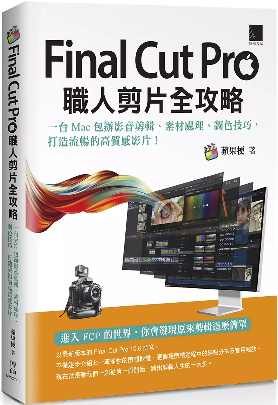
Final Cut Pro職人剪片全攻略:一台 Mac 包辦影音剪輯、素材處理、調色技巧,打造流暢的高質感影片!
為了解決Final Cut Pro 的問題,作者蘋果梗 這樣論述:
拍片很辛苦,剪輯更要有耐心 已經學會iMovie的你,更需要FCP進階技巧,讓每一顆鏡頭都不浪費 進入FCP的世界,你會發現原來剪輯這麼簡單 以最新版本的Final Cut Pro 10.6撰寫。 不僅逐步介紹此一革命性的剪輯軟體,更傳授剪輯過程中的經驗分享及實用祕訣。 現在就跟著我們一起從第一頁開始,跨出剪輯人生的一大步。 Final Cut Pro 一直都是業界最受歡迎的影片剪輯軟體之一。身為專業非線性剪輯軟體的 Final Cut Pro,自從推出 Final Cut Pro X 之後,因為介面與 iMovie 非常類似,吸引了不少使用
者願意開始學習。但是由於多年來沒有繁體中文版本,讓許多人在入門時遇到了不少挫折。 然而儘管剪輯的節奏與美感,是需要天份和更多的經驗累積。但絕對不應該卡在第一步「不知道怎麼使用軟體」。現在就開始打破第一步,拿起本書一起進入 Final Cut Pro 剪輯的有趣世界。 本書作者發揮蘋果教育訓練多年的經驗,從最基礎的介面介紹到實務上的經驗談,一步步的系統化教學,讓每位讀者都能學到許多不為人知的技巧,獨當一面的使用 Final Cut Pro 進行剪輯。 本書特色 ⚙革命性的剪輯方式 ⚙整理素材、剪輯、調色、輸出,一氣呵成 ⚙飛快的專業級效能 ⚙豐富的外掛資源
Final Cut Pro進入發燒排行的影片
訂閱阿宅爸爸的影片 https://tinyurl.com/y9w99rf6
===========================
0歲兒扶著沙發成功站起來了卻...
7年前了,時間過的好快啊!
桐7m13d
5年後..跌倒了不斷站起來學直排輪:
https://youtu.be/gRzHbPnssh4
同場加映,弟弟也扶著同一張無印良品沙發突然就站起來了(咚7m4d):
https://youtu.be/9Vwn_HG4ohk
謝謝您在茫茫人海中點閱我們的影片,
YouTube每天有成千上萬隻影片上傳,實在是難得的緣份,極有可能是一期一會,
歡迎訂閱我們的頻道,常常來看新影片。
如果喜歡我們,覺得影片不錯,也請不要吝嗇幫我們按一個👍讚,
對於我們是莫大的鼓勵,謝謝您
阿宅爸爸的FB跟IG
FB: https://www.facebook.com/otaku.father/
IG: otaku.father https://www.instagram.com/otaku.father
===========================
拍攝工具:
Samsung S10+
GoPro Hero 8
SONY RX100M5A
===========================
剪輯工具:
iMovie
final cut pro
===========================
我的mail:
[email protected]
===========================
幸福有沒有在我身邊,怎麼一直看不見~
爸爸說幸福就在鏡子裡,那就是我快樂的臉~
Precision nutrition for children with early puberty: leveraging nutrigenomics and lipidomics analysis
為了解決Final Cut Pro 的問題,作者NGAN THI KIM NGUYEN 這樣論述:
Background: Precocious puberty (PP) is puberty occurring at an unusually early age that brings in adverse health outcomes during adolescence and adulthood. Pubertal development is a complex biological process of sexual development and is affected by genetic, nutritional, environmental, and socio-ec
onomic factors. However, the relationship between pre-pubertal intakes of energy, fat, fiber, protein levels and pubertal timing has been debated. In the genomic era, it is necessary to examine the individual response to a specific diet and how diet influences metabolic regulation in children with P
P personally. Limited evidence investigated the timing of pubertal onset by examining the interaction of nutrient intake and PP-related genetic loci. Importantly, endocrine disorders can alter lipid metabolism. The fact that puberty onset requires critical weight and body fat based on the “critical
weight hypothesis” and many lipid species have been noticed in many human obesity and metabolic syndrome studies. However, a lack of evidence works on lipidomes to propose the based-lipid biomarker and lipid metabolism in predicting PP in children.Methods: By performing a systematic review and meta-
analysis of prospective studies, we aimed to disclose the role of pre-pubertal and pubertal nutrient intake in PP development. Thereafter, we conducted a Taiwan Puberty Longitudinal Study (TPLS) in recruiting adolescents from pubertal and pediatric endocrine clinics in the Northern/Southern part of
Taiwan. The buccal samples for deoxyribonucleic acid (DNA) extraction and genotyping were collected from a total of 1404 children. We will examine the nutrient intake on the interaction with PP-related SNPs on pubertal timing using the “interaction term” of logistic regression. Also, lipidomic analy
sis deriving from 178 subjects’ plasma samples was used to identify the critical lipid biomarkers in diagnosing PP and central precocious puberty (CPP).Results: A high intake of protein, particularly animal protein, monounsaturated fatty acids (MUFAs), polyunsaturated fatty acids (PUFAs) among prepu
bertal girls were significantly associated with PP risk. We also found that SNP rs12617311, rs2090409, and rs12148769 were significantly associated with PP in children. Specifically, different genotypes interacted with such food groups and micronutrient intake. A significant interaction was observed
between intake of vegetables, fruits, fructose and menarcheal loci rs12617311 (PCL1). The rs2090409 (TMEM38B) was more likely to interact with vitamin intake. Importantly, rs12148769 (MKRN3) appeared a significant interaction with saturated FA and MUFA intake. Whist, SNP rs10980921 (ZNF483) showed
a significant interaction with total PUFAs intake. The intake of sucrose, MUFAs, and PUFAs was associated with the potential lipid-based biomarkers, such as Cer(d16:1/22:0), PI(18:2/22:1), and PI(18:2/22:2) of girls and Cer(t20:0/18:0), Cer(d18:1/16:0) and Cer(d18:1/18:1) of boys that could predict
PP and CPP onset. In addition, the lipidomic analysis proposed several candidate lipids metabolism pathways, such as sphingolipid metabolism, steroid biosynthesis, and bile acid biosynthesis for an in-depth lipid mechanism that can be linked to PP and CPP pathophysiology.Conclusion: There was an int
eraction between genetic variant, lipid metabolism, and nutrient intake that was convinced to be associated with PP and CPP development in girls and boys. Nutrient intake may be an important factor in modulating early puberty, especially the consumption of sugar, fructose, and specific saturated fat
ty acids, monounsaturated fatty acids, polyunsaturated fatty acids. Additional research is needed to determine the biological causes of individual variability in response to dietary intake. Likewise, understanding the influence of nutrigenetic interactions on dyslipidemia can aid in the development
and implementation of personalized dietary strategies to improve the PP and CPP treatment.
Logic Pro X - Apple Pro Training Series

為了解決Final Cut Pro 的問題,作者Nahmani, David 這樣論述:
The Apple-Certified Way to Learn Record, arrange, produce, mix, and master music with this bestselling, Apple-certified guide to Logic Pro. Veteran producer and composer David Nahmani uses real-world professional Logic Pro projects to guide you through step-by-step instructions and straightforwar
d explanations, ranging from basic music creation to sophisticated production techniques.You’ll trigger Live Loops in real time, record audio and software instruments, create and edit sequences, and build arrangements. You’ll create both acoustic and electronic virtual drum performances. You’ll use
Quick Sampler to create stutter effects and vocal chop, and explore ear candy production techniques, such as parallel processing and turntable start and stop effects. You’ll use Smart Controls to map knobs, buttons, and drum pads on a MIDI controller or an iPad. You’ll harness the power of Smart Tem
po to sync up all your audio and MIDI. You’ll use Flex Time to stretch audio and correct the timing of recordings, and you’ll tune vocals with Flex Pitch. You’ll mix, automate, and master the song with EQ, compression, delay, reverb, limiters, and other plug-ins to achieve a professional sound. Fina
lly, you’ll create a 3D spatial audio mix with Logic Pro’s new Dolby Atmos plug-ins, using binaural rendering to experience that immersive sonic experience on your headphones.Downloadable real-world, professional Logic projectsStep-by-step hands-on exercisesAccessible writing style that puts an expe
rt mentor at your sideAmple illustrations that help you quickly master techniquesLists of keyboard shortcuts used in each lessonTips to improve your workflowOnline personal support on the author’s websiteThe Apple Pro Training Series is Apple’s official self-paced learning resource. Books in this se
ries offer downloadable lesson files and an online version of the book. Additional information on this and other books in this series can be found at peachpit.com/apple. For more on certification, visit training.apple.com.Also in the Apple Pro Training Series: Final Cut PromacOS Support Essentials
低功耗高性能電流式感測放大器設計
為了解決Final Cut Pro 的問題,作者梁文顏 這樣論述:
Table of ContentsRecommendation Letters from Thesis AdvisorsThesis/Dissertation Oral Defense Committee CertificationPreface iiiAbstract ivTable of Contents vList of Figures viiList of Tables xiChapter 1 Introduction 11.1 Memory and Processors 21.2 Sense Amplifiers 31.3 Technology Trends 41.4 Circui
t Trends 51.5 Other Trends 61.6 SRAM Trends 71.7 Associated Challenges 9Chapter 2 A Circuits Survey 102.1 The Two Broad Classes 102.2 Voltage Sensing 122.3 Current Sensing 162.4 Others 20Chapter 3 Development of a Three-Transistor I–V Converter 223.1 Low Drop-Out Voltage Regulator as a I–V Converter
233.2 I–V Converter as a Current Sense Amplifier 253.3 Simplifying the I–V Converter 253.4 Proof of Concept 273.5 Quest for a Better Error Amplifier 293.6 Revisiting the Proof of Concept 31Chapter 4 Implementation of a Current Sense Amplifier 344.1 Sense Amplifier Shut-Down 344.2 Static Power Reduc
tion 364.3 Pulsed Word-Line Operation 374.4 Bit-Line Capacitance—Effect on Delay 394.5 Bias Variation 414.6 Relevant Concerns 43Chapter 5 Conclusion 445.1 Simulation Results 445.2 Considerations for Long Bit-Lines 465.3 Measurements 475.4 Derivative Circuits 495.5 Derivative Use 525.6 Summary 555.7
Final Thoughts 55References 56Appendices 83List of FiguresFigure 1.1 Die micrograph from [Singh et al., 2018] 2Figure 1.2 Layout from [Takemoto et al., 2020] 2Figure 1.3 Package from [Poulton et al., 2019] 4Figure 1.4 Wearable for happiness index from [Yano et al., 2015] 6Figure 1.5 Test chip from [
Song et al., 2017] 7Figure 2.1 Left–right: nMOS common-source, -gate and -drain amplifier configurations 10Figure 2.2 Left–right: pMOS common-drain, -gate and -source amplifier configurations 11Figure 2.3 Bi-stable constructed of two inverters 11Figure 2.4 Regenerative latch transient simulation out
put 11Figure 2.5 nMOS differential pair 12Figure 2.6 nMOS–input pair differential amplifier 13Figure 2.7 Clocked latch with isolation 14Figure 2.8 Current-controlled latch 15Figure 2.9 Left–right: Resistor and nMOS approximates 16Figure 2.10 Left–right: Resistor and pMOS approximates 16Figure 2.11 n
-p-n common-base amplifier 17Figure 2.12 Partial schematic from [Yeo and Rofail, 1995] 17Figure 2.13 Left–right: nMOS and pMOS current mirrors 18Figure 2.14 Current sense amplifier from [Ishibashi et al., 1995] 18Figure 2.15 Current sense amplifier from [Seno et al., 1993] 19Figure 2.16 Current conv
eyor from [Seevinck et al., 1991] 19Figure 2.17 pMOS-neutralised nMOS differential pair 20Figure 2.18 Λ-type negative resistance from [Wu and Lai, 1979] 21Figure 2.19 I D -V D characteristic of the Λ-type negative resistance 21Figure 3.1 Three-transistor I–V converter 22Figure 3.2 Simplified low dro
p-out voltage regulator 23Figure 3.3 Low drop-out voltage regulator configured as a I–V converter 24Figure 3.4 Low drop-out voltage regulator as a current sense amplifier 25Figure 3.5 Reference-free I–V converter 26Figure 3.6 Logic inverters as positive-gain amplifier 26Figure 3.7 Proof of concept d
esign 27Figure 3.8 Proof of concept design transient simulation output 28Figure 3.9 Typical and unintended input(s) of the logic inverter 29Figure 3.10 Normalised absolute gain plot for each inverter input 30Figure 3.11 Connections made for the absolute gain plot 30Figure 3.12 Bias generator for the
absolute gain plot 31Figure 3.13 Error amplifier replacement in the proof of concept design 31Figure 3.14 Three-transistor I–V converter 32Figure 3.15 Corresponding bias generator of Figure 3.14 32Figure 3.16 Simulation circuit for verifying the improved error amplifier 33Figure 3.17 Demonstration
of the three-transistor I–V converter as a current sense amplifier 33Figure 4.1 Actions to achieve desired node characteristics during shut-down 34Figure 4.2 Figure 3.14 modified for shut-down 35Figure 4.3 Corresponding bias generator of Figure 4.2 35Figure 4.4 Shared use of bias generator 36Figure
4.5 Pseudo-differential version of Figure 4.4 37Figure 4.6 Pseudo-differential configuration of Figure 3.14 37Figure 4.7 Pulsed read of a ZERO 38Figure 4.8 Pulsed read of a ONE 38Figure 4.9 Differential development across dynamic bit-lines and csa outputs 39Figure 4.10 Delay behaviour with capacitiv
e bit-line loading 40Figure 4.11 Normalised csa bias current variation with supply voltage 41Figure 4.12 Normalised csa bias current variation with temperature 42Figure 4.13 Mismatch view of Figure 3.14 43Figure 5.1 Test set-up (external trigger connection not drawn) 47Figure 5.2 Oscillogram demonst
rating circuit functionality at VDD = 2.55V 47Figure 5.3 Test set-up photograph 48Figure 5.4 Left–right: Three-transistor I–V converter and its complement 49Figure 5.5 Transfer characteristics of the circuits in Figure 5.4 49Figure 5.6 Four-transistor I–V converter 50Figure 5.7 Corresponding bias ge
nerator of Figure 5.6 50Figure 5.8 Impact of sizing on AC performance 51Figure 5.9 Left–right: V SS -, V DD -referenced and floating optical receiver front ends 52Figure 5.10 Transfer characteristic of floating I–V converter 53Figure 5.11 High output resistance eases filter realisation 53Figure 5.12
Three-transistor I–V converter operating as an open-drain receiver 54Figure A.1 inv symbol 84Figure A.2 Alternate inv symbol 84Figure A.3 inv transistor-level schematic 84Figure A.4 inv4 symbol 85Figure A.5 inv4 transistor-level schematic 85Figure A.6 inv16 symbol 86Figure A.7 inv16 transistor-leve
l schematic 86Figure A.8 nand2 symbol 87Figure A.9 nand2 transistor-level schematic 87Figure A.10 nand2b symbol 88Figure A.11 nand2b gate-level schematic 88Figure A.12 nor2 symbol 89Figure A.13 nor2 transistor-level schematic 89Figure A.14 nor2b symbol 90Figure A.15 nor2b gate-level schematic 90Figu
re A.16 or2 symbol 91Figure A.17 or2 gate-level schematic 91Figure A.18 tinv symbol 92Figure A.19 tinv transistor-level schematic 92Figure A.20 dlat symbol 93Figure A.21 dlat gate-level schematic 93Figure A.22 dlatr symbol 94Figure A.23 dlatr gate-level schematic 94Figure A.24 dlats symbol 95Figure
A.25 dlats gate-level schematic 95Figure A.26 tie0 symbol 96Figure A.27 tie0 transistor-level schematic 96Figure A.28 tie1 symbol 97Figure A.29 tie1 transistor-level schematic 97Figure B.1 bit0 symbol 99Figure B.2 bit0 transistor-level schematic 99Figure B.3 bit1 symbol 100Figure B.4 bit1 transistor
-level schematic 100Figure B.5 blrc symbol 101Figure B.6 blrc cell-level schematic 101Figure B.7 pre symbol 102Figure B.8 pre transistor-level schematic 102Figure B.9 rblrc symbol 103Figure B.10 rblrc cell-level schematic 103Figure B.11 wr symbol 104Figure B.12 wr transistor-level schematic 105Figur
e B.13 anand2 symbol 106Figure B.14 Alternate anand2 symbol 106Figure B.15 anand2 transistor-level schematic 107Figure B.16 ckgen symbol 108Figure B.17 ckgen gate-level schematic 108Figure B.18 peri symbol 109Figure B.19 peri cell-level schematic 110Figure B.20 csa symbol 111Figure B.21 csa transist
or-level schematic 111Figure B.22 kobl symbol 112Figure B.23 Alternate kobl symbol 112Figure B.24 kobl transistor-level schematic 113Figure B.25 kobs symbol 114Figure B.26 kobs transistor-level schematic 114Figure C.1 sram1 symbol 116Figure C.2 sram1 block-level schematic 117Figure C.3 sram2 symbol
118Figure C.4 sram2 block-level schematic 119Figure C.5 sram3 symbol 120Figure C.6 sram3 block-level schematic 121Figure D.1 ainvl symbol 123Figure D.2 ainvl transistor-level schematic 123Figure D.3 ainvs symbol 124Figure D.4 Alternate ainvs symbol 124Figure D.5 ainvs transistor-level schematic 124F
igure D.6 cut symbol 125Figure D.7 cut cell-level schematic 126Figure D.8 inAmp symbol 127Figure D.9 inAmp cell-level schematic 127Figure D.10 CD4007 symbol 128Figure D.11 CD4007 transistor-level schematic 128Figure D.12 LF356 symbol 129Figure D.13 LF356 cell-level schematic 129Figure D.14 TL431 sym
bol 130Figure D.15 TL431 cell-level schematic 130Figure D.16 tialp symbol 131Figure D.17 tialp transistor-level schematic 131Figure D.18 tiasd symbol 132Figure D.19 tiasd transistor-level schematic 132Figure D.20 tiasn symbol 133Figure D.21 tiasn transistor-level schematic 133Figure D.22 tiasp symbo
l 134Figure D.23 tiasp transistor-level schematic 134Figure E.1 nfet and equivalent nMOS symbol 135Figure E.2 pfet and equivalent pMOS symbol 136Figure E.3 Circuit for estimating per-bit junction capacitance 137Figure E.4 Simulation output for estimating per-bit junction capacitance 138Figure E.5 Ci
rcuit for estimating per-bit bit-line leakage current 138Figure E.6 ID-VD characteristics 139Figure E.7 ID-VG characteristics 140Figure E.8 anand2 transistor-level schematic 141Figure E.9 Test board functional blocks 144Figure E.10 Test board block-level schematic 145Figure E.11 Signal source connec
ted to abbreviated input network 148Figure E.12 General form of a typical instrumentation amplifier 150Figure E.13 Inverting integrator section of test board 154List of TablesTable 1.1 Semiconductor memory hierarchy 1Table 5.1 Column height h = 512b 44Table 5.2 Column height h = 1Kb 44Table 5.3 Colu
mn height h = 2Kb 44Table 5.4 Summarised measurement results 48Table A.1 List of standard cells 83Table A.2 inv truth table 84Table A.3 inv4 truth table 85Table A.4 inv16 truth table 86Table A.5 nand2 truth table 87Table A.6 nand2b truth table 88Table A.7 nor2 truth table 89Table A.8 nor2b truth tab
le 90Table A.9 or2 truth table 91Table A.10 tinv truth table 92Table A.11 dlat truth table 93Table A.12 dlatr truth table 94Table A.13 dlats truth table 95Table A.14 tie0 truth table 96Table A.15 tie1 truth table 97Table B.1 List of custom cells 98Table B.2 pre truth table 102Table B.3 wr truth tabl
e 104Table C.1 SRAM cells and read path configurations 115Table D.1 List of other cells 122Table E.1 Transistor performance 140Table E.2 Primary bill of materials 146Table E.3 Additional hardware 147Table E.4 List of instruments 155Table F.1 List of abbreviations 158Table F.2 List of symbols 159Tabl
e F.3 List of AC quantities 160Table F.4 List of DC quantities 161Table F.5 List of partial-swing signals 162Table F.6 List of rail–rail signals 162Table F.7 List of instance names 163