pcie ssd的問題,透過圖書和論文來找解法和答案更準確安心。 我們找到下列懶人包和總整理
pcie ssd的問題,我們搜遍了碩博士論文和台灣出版的書籍,推薦李志明,吳國安,李翔寫的 Intel大師帶你架設AI底層:持久記憶體架構服務實作 和林銘波的 微算機原理與應用:x86/x64微處理器軟體、硬體、界面與系統(第六版)(精裝本)都 可以從中找到所需的評價。
另外網站了解SSD 技術:NVMe、SATA、M.2也說明:NVMe (非揮發性記憶體通訊協定) 是一種驅動PCIe 介面固態硬碟的通訊協定。透過定義一套指令集和功能集,以提高各個企業和用戶端系統的效能和互通性。 NVMe 專為SSD 所 ...
這兩本書分別來自深智數位 和全華圖書所出版 。
長庚大學 奈米工程及設計碩士學位學程 周煌程、杨杰圣所指導 梁文顏的 低功耗高性能電流式感測放大器設計 (2020),提出pcie ssd關鍵因素是什麼,來自於電流式電路、感測放大器。
而第二篇論文國立臺灣大學 電子工程學研究所 闕志達所指導 劉雨東的 基於FPGA的多精度神經網路推理加速系統 (2020),提出因為有 機器學習、卷積神經網路、多精度神經網路、量化神經網路、推論加速系統、FPGA的重點而找出了 pcie ssd的解答。
最後網站M.2 PCIE SSD 速度的迷思則補充:我個人是從SATA SSD 升級成M.2 PCIE SSD 說實在的... 感覺都是"一樣快"這是之前的SATA SSD Intel 520 (操了快五年還是頭好壯壯)這是現在的M.2 PCIE ...
Intel大師帶你架設AI底層:持久記憶體架構服務實作
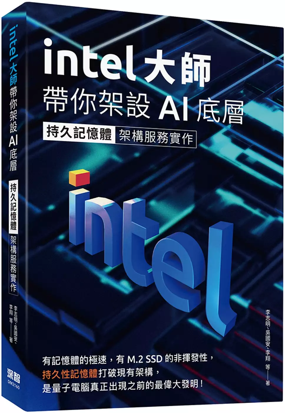
為了解決pcie ssd 的問題,作者李志明,吳國安,李翔 這樣論述:
有記憶體的極速,有M.2 SSD的非揮發性, 持久性記憶體打破現有架構,是量子電腦真正出現之前的最偉大發明! Intel作者群帶你進入持久化記憶體的世界 分層記憶體架構是現代電腦的基石,從CPU之內的L1、L2、L3快取以降,一直到DDR4/5的主記憶體,速度從快到慢,但真正阻礙電腦速度的最大瓶頸,就是下一層的非揮發性儲存了。雖然PCIE Gen4的M.2 SSD已達到7000MB/s的驚人讀取速度,但和處理器內的記憶體來說還是有1000倍以上的差距。為了彌補這個鴻溝,Intel推出了全新的記憶體架構,再揮發性記憶體子系統和發揮發性儲存系統之間,新增了一個新的層次,既能滿足高速的記
憶體資料傳輸,又能保有可儲存性的優點,這個稱之為3D-XPoint的技術,再度造成了整個電腦系統的世代革命。當電腦的主架構發生了天翻地覆的改變時,應用程式、伺服器、資料庫、大數據、人工智慧當然也出現了必需性的變化。在設計巨量資料的服務系統時,傳統針對記憶體斤斤計較的場景不再出現,取代的是大量運用新的持久性記憶體架構來降低系統I/O的頻寬。這對新一代的雲端運算資料中心的影響更是巨大。包括了虛擬機、容器、進而對於應用程式如軟體開發、資料庫、NoSQL、SAP/Hana,Hadoop/Spark也產生了巨大的影響。 本書是國內第一本中文說明這種新型應用的書籍,閱讀本書之後,對大型系統的運維已
不再是TB級而達到PB的記憶體等級了,想想一個巨型的系統服務不需要水平擴充(Scale-out)r而是可以垂直擴充(Scale-up),這完全打破了我們從前的概念,本書將是你在進入量子電腦世代來臨前最迫切需要獲得的知識。 本書特色 1.在英特爾公司任職的多位專家們齊聚一堂,共同創作了這本持久化記憶體的實戰書籍。 2.仔細講解、深入淺出,搭配圖表輔助說明,好看好讀好吸收。 3.台灣第一本詳細解說持久記憶體的電腦書,讓你迅速精進,保持業界頂峰的地位。 名人推薦 「借助英特爾傲騰持久記憶體,我們在記憶體--儲存子系統中創建了一個新層次,這使整個產業都會受益。持久記憶體
基於革命性的英特爾3D-XPoint 技術,將傳統記憶體的速度與容量和持久性結合在一起。」──阿爾珀·伊爾克巴哈(Alper Ilkbahar),英特爾公司資料平台事業部副總裁、記憶體和儲存產品事業部總經理
pcie ssd進入發燒排行的影片
感謝 @ASUS 的邀約,讓我有機會體驗全球大缺貨的 ZenBook Duo 14 (UX482)。
我覺得最神奇的是雙螢幕的應用,
把筆電下方的空間用好用滿。
在資訊爆炸的時代,多一塊 ScreenPad Plus,工作效率翻倍。
雖然幾年前 ASUS 就推出了雙螢幕筆電,
但實際使用起來還是為之驚艷。
外觀設計質感爆棚、
效能表現足以應付 1080P 的輕度創作者、
豐富的 I/O 連接埠包括 Micro SD、Thunderbolt 4 等,
14 吋 16.9mm 1.6kg 方便攜帶、
完全針對輕度創作斜槓青年推出的輕薄筆電。
詳細使用體驗分享,歡迎觀看完整版影片 =)
#ASUS #ZenBook_Duo_14 #雙螢幕筆電 #雙倍效率 #斜槓青年
【產品規格】
- 最高搭載Intel® Core™ i7 處理
- NVIDIA® GeForce® MX450 獨立顯示卡
- AAS雙風扇設計
- 32G RAM
- 1Tb PCIe SSD
【產品資訊】
品牌:ASUS
型號:ZenBook Duo 14 (UX482)
了解更多:https://bit.ly/3i0yjG3
00:00 前言
00:58 特寫畫面
01:07 外觀設計
02:54 I/O 連接埠
04:31 規格
05:37 使用體驗
07:56 ScreenPad Plus 功能
10:38 效能使用心得
11:27 其他功能
11:54 結論
►歡迎加入 Telegram ►
打倒演算法的高牆? https://t.me/alvinist
►本集使用音樂►
* 行動派艾草之後可以到「社群」查看專屬貼文下載音樂。
▶行動派艾草▶ 頻道會員持續募集中
▉「行動派艾草」是什麼?
這是 YouTube 推出的「定期型群眾募資」。
俗氣的說,就是:用錢支持喜歡的創作者。
可依照自己的能力,選擇支持方案。
行動派艾草 / 每個月 75 元(新台幣);
銀級行動派艾草 / 每個月 450 元(新台幣);
金級行動派艾草 / 每個月 900 元(新台幣);
尊爵行動派艾草 / 每個月 1,600 元(新台幣)。
YouTube 將抽取三成費用。
其餘的將提供給創作者,(希望可以)無憂無慮的創作、添購設備器材等。
點選以下網址,綁定信用卡即可:
https://www.youtube.com/alvinist/join
►艾爾文的社群 / 歡迎追蹤►
▎所有社群平台連結:https://linktr.ee/Alvinist
▎Telegram 官方公告頻道: https://t.me/alvinist
▎YouTube 子頻道:http://youtube.com/coopaler
▎Instagram 很精彩: http://www.instagram.com/alvinist
▎Facebook 粉絲專頁: http://www.facebook.com/alvinistvlog
▎Twitter 偶爾更新: http://www.twitter.com/alvinist
►艾耳聞 Podcast 博客收聽平台►
▎Apple Podcasts: https://apple.co/2RVWA36
▎Spotify Podcasts: https://spoti.fi/3eDkytP
▎Google Podcasts: https://bit.ly/3bxKkgS
▎SoundOn 及 KKbox 請搜尋「艾爾文」
►我的器材 / My Gear►
https://kit.co/Alvinist
►合作請洽►
[email protected]
►親愛的艾爾文時間► 信件及包裹寄送地址
【中文】23599 中和宜安郵局第 171 號信箱
【英文】P.O.BOX 171 Zhonghe Yi-an, New Taipei City, 23599 Taiwan (R.O.C)
低功耗高性能電流式感測放大器設計
為了解決pcie ssd 的問題,作者梁文顏 這樣論述:
Table of ContentsRecommendation Letters from Thesis AdvisorsThesis/Dissertation Oral Defense Committee CertificationPreface iiiAbstract ivTable of Contents vList of Figures viiList of Tables xiChapter 1 Introduction 11.1 Memory and Processors 21.2 Sense Amplifiers 31.3 Technology Trends 41.4 Circui
t Trends 51.5 Other Trends 61.6 SRAM Trends 71.7 Associated Challenges 9Chapter 2 A Circuits Survey 102.1 The Two Broad Classes 102.2 Voltage Sensing 122.3 Current Sensing 162.4 Others 20Chapter 3 Development of a Three-Transistor I–V Converter 223.1 Low Drop-Out Voltage Regulator as a I–V Converter
233.2 I–V Converter as a Current Sense Amplifier 253.3 Simplifying the I–V Converter 253.4 Proof of Concept 273.5 Quest for a Better Error Amplifier 293.6 Revisiting the Proof of Concept 31Chapter 4 Implementation of a Current Sense Amplifier 344.1 Sense Amplifier Shut-Down 344.2 Static Power Reduc
tion 364.3 Pulsed Word-Line Operation 374.4 Bit-Line Capacitance—Effect on Delay 394.5 Bias Variation 414.6 Relevant Concerns 43Chapter 5 Conclusion 445.1 Simulation Results 445.2 Considerations for Long Bit-Lines 465.3 Measurements 475.4 Derivative Circuits 495.5 Derivative Use 525.6 Summary 555.7
Final Thoughts 55References 56Appendices 83List of FiguresFigure 1.1 Die micrograph from [Singh et al., 2018] 2Figure 1.2 Layout from [Takemoto et al., 2020] 2Figure 1.3 Package from [Poulton et al., 2019] 4Figure 1.4 Wearable for happiness index from [Yano et al., 2015] 6Figure 1.5 Test chip from [
Song et al., 2017] 7Figure 2.1 Left–right: nMOS common-source, -gate and -drain amplifier configurations 10Figure 2.2 Left–right: pMOS common-drain, -gate and -source amplifier configurations 11Figure 2.3 Bi-stable constructed of two inverters 11Figure 2.4 Regenerative latch transient simulation out
put 11Figure 2.5 nMOS differential pair 12Figure 2.6 nMOS–input pair differential amplifier 13Figure 2.7 Clocked latch with isolation 14Figure 2.8 Current-controlled latch 15Figure 2.9 Left–right: Resistor and nMOS approximates 16Figure 2.10 Left–right: Resistor and pMOS approximates 16Figure 2.11 n
-p-n common-base amplifier 17Figure 2.12 Partial schematic from [Yeo and Rofail, 1995] 17Figure 2.13 Left–right: nMOS and pMOS current mirrors 18Figure 2.14 Current sense amplifier from [Ishibashi et al., 1995] 18Figure 2.15 Current sense amplifier from [Seno et al., 1993] 19Figure 2.16 Current conv
eyor from [Seevinck et al., 1991] 19Figure 2.17 pMOS-neutralised nMOS differential pair 20Figure 2.18 Λ-type negative resistance from [Wu and Lai, 1979] 21Figure 2.19 I D -V D characteristic of the Λ-type negative resistance 21Figure 3.1 Three-transistor I–V converter 22Figure 3.2 Simplified low dro
p-out voltage regulator 23Figure 3.3 Low drop-out voltage regulator configured as a I–V converter 24Figure 3.4 Low drop-out voltage regulator as a current sense amplifier 25Figure 3.5 Reference-free I–V converter 26Figure 3.6 Logic inverters as positive-gain amplifier 26Figure 3.7 Proof of concept d
esign 27Figure 3.8 Proof of concept design transient simulation output 28Figure 3.9 Typical and unintended input(s) of the logic inverter 29Figure 3.10 Normalised absolute gain plot for each inverter input 30Figure 3.11 Connections made for the absolute gain plot 30Figure 3.12 Bias generator for the
absolute gain plot 31Figure 3.13 Error amplifier replacement in the proof of concept design 31Figure 3.14 Three-transistor I–V converter 32Figure 3.15 Corresponding bias generator of Figure 3.14 32Figure 3.16 Simulation circuit for verifying the improved error amplifier 33Figure 3.17 Demonstration
of the three-transistor I–V converter as a current sense amplifier 33Figure 4.1 Actions to achieve desired node characteristics during shut-down 34Figure 4.2 Figure 3.14 modified for shut-down 35Figure 4.3 Corresponding bias generator of Figure 4.2 35Figure 4.4 Shared use of bias generator 36Figure
4.5 Pseudo-differential version of Figure 4.4 37Figure 4.6 Pseudo-differential configuration of Figure 3.14 37Figure 4.7 Pulsed read of a ZERO 38Figure 4.8 Pulsed read of a ONE 38Figure 4.9 Differential development across dynamic bit-lines and csa outputs 39Figure 4.10 Delay behaviour with capacitiv
e bit-line loading 40Figure 4.11 Normalised csa bias current variation with supply voltage 41Figure 4.12 Normalised csa bias current variation with temperature 42Figure 4.13 Mismatch view of Figure 3.14 43Figure 5.1 Test set-up (external trigger connection not drawn) 47Figure 5.2 Oscillogram demonst
rating circuit functionality at VDD = 2.55V 47Figure 5.3 Test set-up photograph 48Figure 5.4 Left–right: Three-transistor I–V converter and its complement 49Figure 5.5 Transfer characteristics of the circuits in Figure 5.4 49Figure 5.6 Four-transistor I–V converter 50Figure 5.7 Corresponding bias ge
nerator of Figure 5.6 50Figure 5.8 Impact of sizing on AC performance 51Figure 5.9 Left–right: V SS -, V DD -referenced and floating optical receiver front ends 52Figure 5.10 Transfer characteristic of floating I–V converter 53Figure 5.11 High output resistance eases filter realisation 53Figure 5.12
Three-transistor I–V converter operating as an open-drain receiver 54Figure A.1 inv symbol 84Figure A.2 Alternate inv symbol 84Figure A.3 inv transistor-level schematic 84Figure A.4 inv4 symbol 85Figure A.5 inv4 transistor-level schematic 85Figure A.6 inv16 symbol 86Figure A.7 inv16 transistor-leve
l schematic 86Figure A.8 nand2 symbol 87Figure A.9 nand2 transistor-level schematic 87Figure A.10 nand2b symbol 88Figure A.11 nand2b gate-level schematic 88Figure A.12 nor2 symbol 89Figure A.13 nor2 transistor-level schematic 89Figure A.14 nor2b symbol 90Figure A.15 nor2b gate-level schematic 90Figu
re A.16 or2 symbol 91Figure A.17 or2 gate-level schematic 91Figure A.18 tinv symbol 92Figure A.19 tinv transistor-level schematic 92Figure A.20 dlat symbol 93Figure A.21 dlat gate-level schematic 93Figure A.22 dlatr symbol 94Figure A.23 dlatr gate-level schematic 94Figure A.24 dlats symbol 95Figure
A.25 dlats gate-level schematic 95Figure A.26 tie0 symbol 96Figure A.27 tie0 transistor-level schematic 96Figure A.28 tie1 symbol 97Figure A.29 tie1 transistor-level schematic 97Figure B.1 bit0 symbol 99Figure B.2 bit0 transistor-level schematic 99Figure B.3 bit1 symbol 100Figure B.4 bit1 transistor
-level schematic 100Figure B.5 blrc symbol 101Figure B.6 blrc cell-level schematic 101Figure B.7 pre symbol 102Figure B.8 pre transistor-level schematic 102Figure B.9 rblrc symbol 103Figure B.10 rblrc cell-level schematic 103Figure B.11 wr symbol 104Figure B.12 wr transistor-level schematic 105Figur
e B.13 anand2 symbol 106Figure B.14 Alternate anand2 symbol 106Figure B.15 anand2 transistor-level schematic 107Figure B.16 ckgen symbol 108Figure B.17 ckgen gate-level schematic 108Figure B.18 peri symbol 109Figure B.19 peri cell-level schematic 110Figure B.20 csa symbol 111Figure B.21 csa transist
or-level schematic 111Figure B.22 kobl symbol 112Figure B.23 Alternate kobl symbol 112Figure B.24 kobl transistor-level schematic 113Figure B.25 kobs symbol 114Figure B.26 kobs transistor-level schematic 114Figure C.1 sram1 symbol 116Figure C.2 sram1 block-level schematic 117Figure C.3 sram2 symbol
118Figure C.4 sram2 block-level schematic 119Figure C.5 sram3 symbol 120Figure C.6 sram3 block-level schematic 121Figure D.1 ainvl symbol 123Figure D.2 ainvl transistor-level schematic 123Figure D.3 ainvs symbol 124Figure D.4 Alternate ainvs symbol 124Figure D.5 ainvs transistor-level schematic 124F
igure D.6 cut symbol 125Figure D.7 cut cell-level schematic 126Figure D.8 inAmp symbol 127Figure D.9 inAmp cell-level schematic 127Figure D.10 CD4007 symbol 128Figure D.11 CD4007 transistor-level schematic 128Figure D.12 LF356 symbol 129Figure D.13 LF356 cell-level schematic 129Figure D.14 TL431 sym
bol 130Figure D.15 TL431 cell-level schematic 130Figure D.16 tialp symbol 131Figure D.17 tialp transistor-level schematic 131Figure D.18 tiasd symbol 132Figure D.19 tiasd transistor-level schematic 132Figure D.20 tiasn symbol 133Figure D.21 tiasn transistor-level schematic 133Figure D.22 tiasp symbo
l 134Figure D.23 tiasp transistor-level schematic 134Figure E.1 nfet and equivalent nMOS symbol 135Figure E.2 pfet and equivalent pMOS symbol 136Figure E.3 Circuit for estimating per-bit junction capacitance 137Figure E.4 Simulation output for estimating per-bit junction capacitance 138Figure E.5 Ci
rcuit for estimating per-bit bit-line leakage current 138Figure E.6 ID-VD characteristics 139Figure E.7 ID-VG characteristics 140Figure E.8 anand2 transistor-level schematic 141Figure E.9 Test board functional blocks 144Figure E.10 Test board block-level schematic 145Figure E.11 Signal source connec
ted to abbreviated input network 148Figure E.12 General form of a typical instrumentation amplifier 150Figure E.13 Inverting integrator section of test board 154List of TablesTable 1.1 Semiconductor memory hierarchy 1Table 5.1 Column height h = 512b 44Table 5.2 Column height h = 1Kb 44Table 5.3 Colu
mn height h = 2Kb 44Table 5.4 Summarised measurement results 48Table A.1 List of standard cells 83Table A.2 inv truth table 84Table A.3 inv4 truth table 85Table A.4 inv16 truth table 86Table A.5 nand2 truth table 87Table A.6 nand2b truth table 88Table A.7 nor2 truth table 89Table A.8 nor2b truth tab
le 90Table A.9 or2 truth table 91Table A.10 tinv truth table 92Table A.11 dlat truth table 93Table A.12 dlatr truth table 94Table A.13 dlats truth table 95Table A.14 tie0 truth table 96Table A.15 tie1 truth table 97Table B.1 List of custom cells 98Table B.2 pre truth table 102Table B.3 wr truth tabl
e 104Table C.1 SRAM cells and read path configurations 115Table D.1 List of other cells 122Table E.1 Transistor performance 140Table E.2 Primary bill of materials 146Table E.3 Additional hardware 147Table E.4 List of instruments 155Table F.1 List of abbreviations 158Table F.2 List of symbols 159Tabl
e F.3 List of AC quantities 160Table F.4 List of DC quantities 161Table F.5 List of partial-swing signals 162Table F.6 List of rail–rail signals 162Table F.7 List of instance names 163
微算機原理與應用:x86/x64微處理器軟體、硬體、界面與系統(第六版)(精裝本)
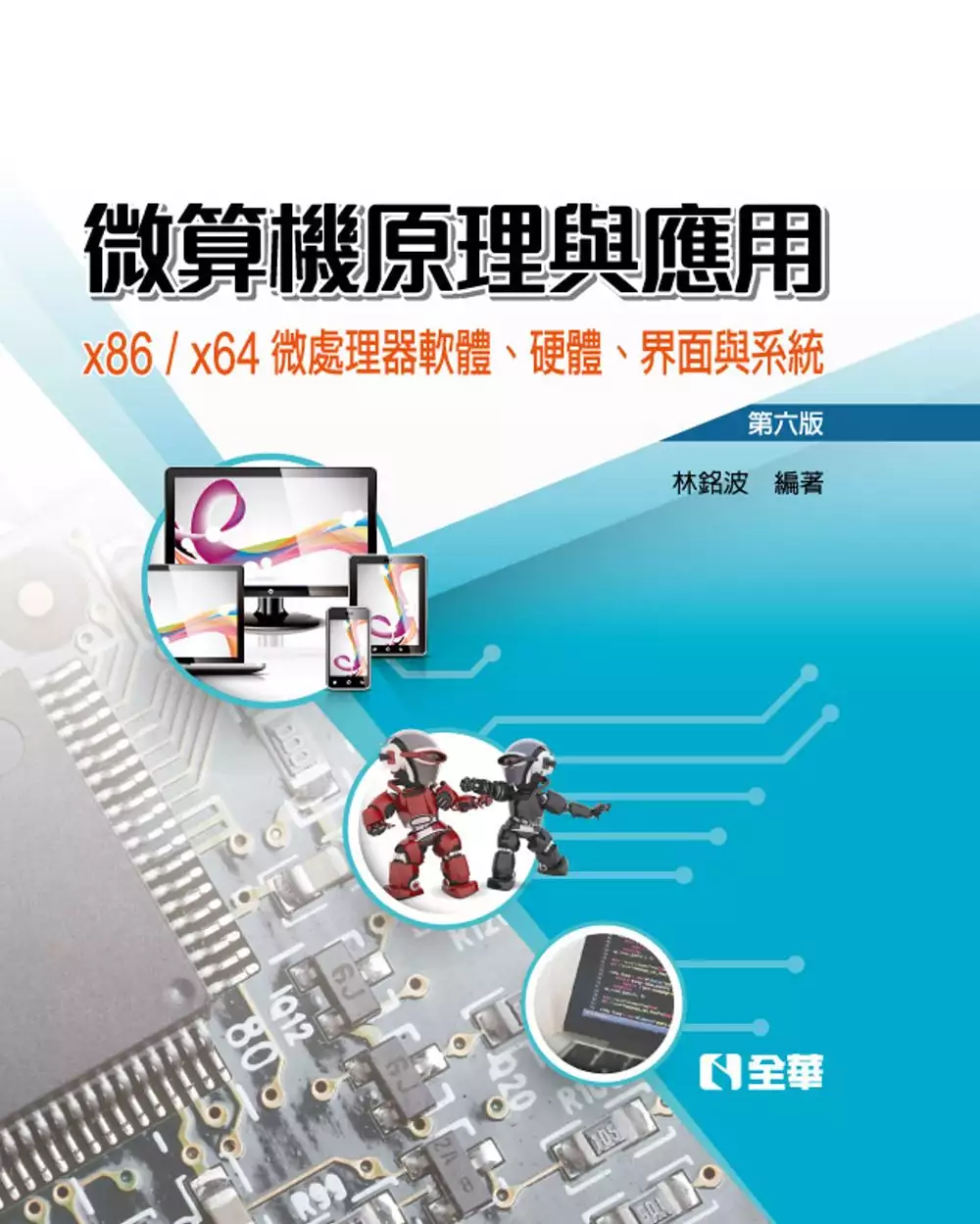
為了解決pcie ssd 的問題,作者林銘波 這樣論述:
微算機原理與應用一書,使用x86與x64微處理器系列為例,期望建立讀者一個完整的微算機原理與相關的基本知識,進而能夠使用與設計各種微處理器系統。由淺入深將x86微處理器的指令分類,並且以豐富的程式實例,闡述每一個指令的動作與應用。相同的分類方法可以引用於學習其它微處理器。 本書特色 1.由淺入深將x86微處理器的指令分類,並且以豐富的程式實例,闡述每一個指令的動作與應用。相同的分類方法可以引用於學習其它微處理器。 2.專章討論8086 CPU的硬體功能、界面、及時序。 3.詳細討論記憶器模組的設計與各種常用的記憶器元件:SRAM、快閃記憶器、DRAM
、SDRAM、及DDR/2/3 SDRAM。 4.專章討論x86的浮點運算(FPU)與多媒體運算(MMX、SSE、SSE2、SSSE3、SSE4)處理器的功能與應用程式設計。 5.專章討論x86 CPU的中斷要求與處理、可規劃中斷要求控制器、及軟體中斷要求指令的應用。 6.詳細介紹I/O觀念與基本結構、I/O資料轉移啟動方式、並列資料轉移、與串列資料轉移。 7.詳細介紹PC系統結構,南橋與北橋晶片組的功能,與單一晶片組PC系統架構。簡要介紹PC系統中的匯流排界面標準(SATA、USB、PCIe、DVI、與HDMI) 8.論述文字模式及繪圖模式螢幕顯示器原理、列表機
原理與界面、磁性記憶器(硬碟)、SSD、與光碟記憶器(CD-ROM、DVD、藍光DVD)。
基於FPGA的多精度神經網路推理加速系統
為了解決pcie ssd 的問題,作者劉雨東 這樣論述:
近年來,神經網路開始被應用在各個領域,如影像辨識、自然語言處理…等,並且都取得了相當不錯的成果。這些研究結果促使了神經網路相關的產品的問世,凸顯了在終端裝置進行神經網路運算的重要性。因此,如何在維持正確率的前提下,以更低的功耗執行更快的神經網路推理運算,便成為了近年研究的重點。本文基於已經被廣泛使用的線性量化技術,引入了更低複雜度的數字格式,並融合了相關研究,提出了完整的混合精度神經網路量化演算法。在各種應用、資料集、模型架構中,我們的演算法都能得到與FP32模型相近的準確率。除此之外,我們也基於此演算法,設計了對應的推理加速電路,並實現在FPGA上。我們的電路不僅支援三種格式的權重,透過i
m2col演算法,更能計算各種參數設定下的卷積神經網路,提升了硬體的使用彈性。最後,我們將演算法、硬體的控制流程與PyTorch進行整合,打造出了一套由量化神經網路訓練到FPGA加速部屬都能支援的完整解決方案。我們在多個神經網路架構中驗證了此系統。平均下來,我們的FPGA的加速系統的運算速度為CPU的2.96倍,能源效率則是CPU的11.43倍。