Coffee a la mode的問題,透過圖書和論文來找解法和答案更準確安心。 我們找到下列懶人包和總整理
Coffee a la mode的問題,我們搜遍了碩博士論文和台灣出版的書籍,推薦ANNECAZOR寫的 創新前衛的分子料理:20種容易理解的技法.40道顛覆味蕾的食譜(暢銷普及版) 和Scarbrough, Mark/ Weinstein, Bruce的 A La Mode: 120 Recipes in 60 Pairings: Pies, Tarts, Cakes, Crisps, and More Topped With Ice Cream, Gelato, Frozen Custard, and M都 可以從中找到所需的評價。
另外網站[邀約]師大‧Cafe a la mode‧聚餐的好地方!招牌法式布丁吐司好好 ...也說明:cafe à la mode 地址:台北市大安區雲和街2-1號電話:02-2362-3957 營業時間:星期一~五10:00am~10:00pm.
這兩本書分別來自積木文化 和所出版 。
長庚大學 電子工程學系 賴朝松所指導 Mamina Sahoo的 基於石墨烯及生物碳基材料的可撓式電晶體應用與能量攫取 (2021),提出Coffee a la mode關鍵因素是什麼,來自於石墨烯、氟化石墨烯、太阳能电池、摩擦纳米发电机、生物碳、能量收集器。
而第二篇論文國立成功大學 建築學系 潘振宇所指導 吳伊証的 高齡日間照顧中心異味樣態調查與新式自然通風效益評估 (2021),提出因為有 異味、日間照顧中心、自然通風、高齡福祉、室內空氣品質的重點而找出了 Coffee a la mode的解答。
最後網站Café à la Mode - Foursquare則補充:Read 8 tips and reviews from 214 visitors about lively, healthy food and cozy. "Great service!"
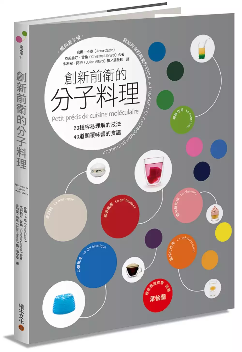
創新前衛的分子料理:20種容易理解的技法.40道顛覆味蕾的食譜(暢銷普及版)
為了解決Coffee a la mode 的問題,作者ANNECAZOR 這樣論述:
分子料理其實一點也不難! 一本掌握關於分子料理的各種原理與活用方式 「科學引領我們探索這個大千世界,研究各種自然現象所引發的不同機制反應,而分子廚藝(Gastronomie Moléculaire)這門學問,即在探究烹飪過程所產生的各種變化,以及人們飲食感官上的普遍現象。這門學問也可以稱作食品科學。技術運用科學知識,提供實務上可行的操作方法。在廚藝相關領域中,烹調技術乃應用分子廚藝及各種食品科學的知識,提出新式的操作方法。廚藝融合了藝術和技術,與味道、產品的品質及廚師的能力皆密不可分;操作和理解實乃一體之兩面,這就是所謂的『分子料理』(Cuisine Moléculaire)。這種料理應
用了廚藝中原有的技巧而創造出新的菜色、新的口感、新的風味、新的感受⋯⋯」——摘自本書p.3簡介 ★寫給所有對美食好奇的人 將食材分子重組變化成形形色色的驚奇創意料理, 輕鬆成為廚房裡的魔法師 所有烹調技法都涵蓋科學原理的簡易說明,搭配簡單有趣、創意十足的料理食譜&精美圖片 像是會在嘴裡迸開的巧克力、甜中帶鹹的蔬菜焦糖、晶瑩剔透的蜂蜜珍珠、口感豐潤的黃瓜優格球、未曾聽聞的醬油泡沫慕斯......甚至,越式湯麵竟成了高湯凍,甜心蛋也能變化成方形或管狀!作法簡單,樣貌驚奇,風味多變,顛覆了我們對廚藝和食材的認知與想像,令人大呼過癮! 本書作者Anne Cazor為「分子廚藝」研究領域的博
士,同時也是「創新料理」(Cuisine Innovation)網站(www.cuisine-innovation.fr)的創辦人。她將這本食譜獻給所有喜愛美食的人,包括業餘老饕和專業廚師。書中針對每道分子料理的烹飪技法,提供相關科學原理的簡易說明,同時搭配兩道讀者可以實地運用、快速上手的食譜,簡單有趣、創意十足,佐以大量精美的圖片,帶給讀者無限的想像空間和前所未有的驚喜。
Coffee a la mode進入發燒排行的影片
7 Eleven Foods Spaghetti Bolognese(meat sauce pasta) and Pudding à la mode. I like 711 meat sauce pasta, so I want to keep it forever!? The Pudding à la mode is classic style,like a old fashioned coffee shop menu.
#japanesestuffchannel, #711food, #pasta
基於石墨烯及生物碳基材料的可撓式電晶體應用與能量攫取
為了解決Coffee a la mode 的問題,作者Mamina Sahoo 這樣論述:
Table of ContentsAbstract.......................................................................................................iFigure Captions........................................................................................xiTable Captions...................................................
....................................xxiChapter 1: Introduction1.1 Flexible electronics................................................................................11.2 Graphene the magical material ………………………….……….......21.2.1 Synthesis of graphene…………………………….….…...21.2.1.1 Mechanical exfoliati
on of graphene………………...……21.2.1.2 Epitaxial growth on Sic substrate………………….…..31.2.1.3 Chemical vapor deposition (CVD) method………….…..41.2.2 Graphene transfer…………………………………………....41.3 Application of graphene based Electronics……………………….......51.3.1 Graphene based flexible transparent electrode
……………….61.3.2 Top gated Graphene field effect transistor…………………….71.4 Challenges of flexible graphene based field effect transistors.……….91.5 Energy harvesting devices for flexible electronics………….........….91.6 Solar cell…………………………………………………………...101.6.1 Device architecture…………………………………………101.
6.2 Issues and Challenges of Perovskite solar cells………...121.7 Triboelectric nanogenerator (TENG)………………………………121.7.1 Working mode of TENG………………………………….141.8 Applications of TENG………………………………………………151.8.1 Applications of graphene based TENG…………………....151.8.2 Applications of bio-waste material ba
sed TENG………….171.9 Key challenges of triboelectric nanogenerator…………………....…191.10 Objective and scope of this study………………………………....19Chapter 2: Flexible graphene field effect transistor with fluorinated graphene as gate dielectric2.1 Introduction………………………………………………………....212.2 Material preparation a
nd Device fabrication………………. 232.2.1CVD Growth of Graphene on Copper Foil………………….232.2.2 Transfer of graphene over PET substrate……………...........252.2.3 Fabrication of fluorinated graphene ……………...........252.2.4 F-GFETs with FG as gate dielectric device fabrication……262.2.5 Material and electrical C
haracterization …………………272.3 Results and discussion…………………………………………….282.3.1 Material characterization of PG and FG……………...…...….282.3.2 Electrical characterization of F-GFET with FG as dielectrics..332.3.3 Mechanical stability test of F-GFET with FG as dielectrics ….362.4 Summary…………………………………………………
………....40Chapter 3: Robust sandwiched fluorinated graphene for highly reliable flexible electronics3.1 Introduction………………………………………………………….423.2 Material preparation and Device fabrication ………………….........443.2.1 CVD Growth of Graphene on Copper Foil…………………...443.2.2 Graphene fluorination …...…….…………
…………..............443.2.3 F-GFETs with sandwiched FG device fabrication....................443.2.4 Material and electrical Characterization…..............................453.3 Results and discussion ……………………………………...............453.3.1 Material characterization of sandwiched…………………….453.3.2 Electric
al characterization of F-GFET with sandwiched FG....473.3.3 Mechanical stability test of F-GFET with sandwiched FG…503.3.4 Strain transfer mechanism of sandwiched FG………………513.4 Summary…………………………………………………………....53Chapter 4: Functionalized fluorinated graphene as a novel hole transporting layer for ef
ficient inverted perovskite solar cells4.1 Introduction………………………………………………………….544.2 Material preparation and Device fabrication......................................564.2.1 Materials ………………………...…………………………564.2.2 CVD-Graphene growth ……………………………...…...564.2.3 Graphene fluorination …………………………………….564.
2.4 Transfer of fluorinated graphene…………………………...574.2.5 Device fabrication …………………………………….….574.2.6 Material and electrical Characterization …….....................584.3 Results and discussion …………………………………………….594.3.1 Surface electronic and optical properties of FGr……….….594.3.2 Characterization o
f FGr and perovskite surface ……….…644.3.3 Electrical performance of PSC………………….…….…...694.3.4 Electrical performance of Flexible PSC……………………724.4 Summary…………………………………………………………...78Chapter 5: Flexible layered-graphene charge modulation for highly stable triboelectric nanogenerator5.1 Introduction…………
…………………………………………....795.2 Experimental Section……………………………………………….825.2.1 Large-area graphene growth ……………………………….825.2.2 Fabrication of Al2O3 as the CTL …………………………...825.2.3 Fabrication of a Gr-TENG with Al2O3 as the CTL………825.2.4 Material characterization and electrical measurements…….835.3 Results
and discussion.…………………………………...…………845.3.1 Material Characterization of Graphene Layers/Al2O3……845.3.2 Working Mechanism of Gr-TENG with Al2O3 as CTL…915.3.3 Electrical Characterization of Gr-TENG with Al2O3 CTL…945.3.4 Applications of the Gr-TENG with Al2O3 as CTL……….1015.4 Summary…………………………………………
……………….103Chapter 6: Eco-friendly Spent coffee ground bio-TENG for high performance flexible energy harvester6.1 Introduction…………………………………………………….......1046.2 Experimental Section…………………………………………….1086.2.1 Material Preparation …………………………………….1086.2.2 Fabrication of SCG powder based TENG………………...1086
.2.3 Fabrication of SCG thin-film based TENG ………………1096.2.4 Material characterization and electrical measurements….1106.3 Results and discussion.…………………………………...………1116.3.1 Material Characterization of SCG powder and thin film….1116.3.2 Working Mechanism of SCG-TENG……………………...1186.3.3 Electrical Cha
racterization of SCG-TENG……………….1226.3.4 Applications of the SCG thin-film based TENG………….1326.4 Summary………………………………………………………….134Chapter 7: Conclusions and future perspectives7.1 Conclusion………………………………………………………....1357.2 Future work …………………………….………………………….1377.2.1 Overview of flexible fluorinated g
raphene TENG..............1377.2.1.1 Initial results………………………………….…1387.2.2.1.1 Fabrication of FG-TENG………………1387.2.2.1.2 Working principle of FG-TENG……….1397.2.2.1.3 Electrical output of FG-TENG.………...140References…………………………………………………………….142Appendix A: List of publications………………….……………..........177A
ppendix B: Fabrication process of GFETs with fluorinated graphene (FG) as gate dielectric……........……………………………………….179Appendix C: Fabrication process of GFETs with sandwiched FG…....180Appendix D: Fabrication process of inverted perovskite solar cell with FGr as HTL…………………………………………………………….181Appendi
x E: Fabrication of a Gr-TENG with Al2O3 as the CTL…….182Appendix F: Fabrication of SCG based triboelectric nanogenerator….183Figure captionsFigure 1-1 Exfoliated graphene on SiO2/Si wafer……………………….3Figure 1-2 Epitaxial graphene growth on SiC substrate………………....3Figure 1-3 Growth mechanism of graphe
ne on Cu foil by CVD ……......4Figure 1-4 Wet transfer process of CVD grown graphene…………...….5Figure 1-5 RGO/PET based electrodes as a flexible touch screen.……....6Figure 1-6 Graphene based (a) touch panel (b) touch-screen phone…….7Figure 1-7 Flexible graphene transistors (a) (Top) Optical photograph
of an array of flexible, self-aligned GFETs on PET. (Bottom) The corresponding schematic shows a device layout. (b) Schematic cross-sectional and top views of top-gated graphene flake–based gigahertz transistors. (Left) AFM image of a graphene flake. (Right) Photograph of flexible graphene devices
fabricated on a PI substrate. (c) Cross-sectional schematic of flexible GFETs fabricated using a self-aligned process……8Figure 1-8 The magnitude of power needed for meet certain operation depending critically on the scale and applications………………………10Figure 1-9 Schematic diagrams of PSC in the (a) n-i
-p mesoscopic, (b) n-i-p planar, (c) p-i-n planar, and (d) p-i-n mesoscopic structures………...12Figure 1-10 Schematic illustration of the first TENG...………………...13Figure 1-11 Working modes of the TENG. (a) The vertical contact-separation mode. (b) The lateral sliding mode. (c) The single-electrode mode
. (d) The free-standing mode ………………………………...……14Figure 1-12 Schematic illustration of (a) device fabrication of graphene-based TENGs (b) graphene/EVA/PET-based triboelectric nanogenerators (c) device fabrication of stretchable CG based TENG with electrical output performance……………………………………………………...17
Figure 1-13 Schematic illustration and output performance of bio-waste material based TENG (a) Rice-husk (b) Tea leaves (c) Sun flower powder (SFP) (d) Wheat stalk based TENG………….…………………………18Figure 2-1 Graphene synthesis by LPCVD method……….…………...24Figure 2-2 Schematic diagram of (a) preparation pro
cess of 1L-FG/copper foil (b) Layer by layer assembly method was used for fabricating three-layer graphene over copper foil and then CF4 plasma treatment from top side to form 3L-FG/copper foil…………………….26Figure 2-3 Schematic illustration of fabrication process of F-GFET with FG as gate dielectric ……
……………………………………………….27Figure 2-4 (a) Raman spectra of PG, 1L-FG and 3L-FG after 30 min of CF4 plasma treatment over copper foil. (b) Peak intensities ratio ID/IG and optical transmittance of PG, 1L-FG and 3L-FG. Inset: image of PG and 1L-FG film over PET substrate. (c) Typical Raman spectra of PG, 1L
-FG and 3L-FG on PET substrate. (d) Optical transmittance of PG, 1L-FG and 3L-FG film over PET substrate. The inset shows the optical image of GFETs with FG as gate dielectrics on PET ……….…………30Figure 2-5 XPS analysis result of (a) PG (b) 1L-FG (c) 3L-FG where the C1s core level and several carbon f
luorine components are labeled. The inset shows the fluorine peak (F 1s) at 688.5 eV……………………….32Figure 2-6 (a) Water contact angle of PG, 1L-FG and 3L-FG over PET substrate. (b) The relationship between water contact angle of PG, 1L-FG and 3L-FG and surface-roughness………………………………………33Figure 2-7 (a) I
d vs. Vd of w/o-FG, w/1L-FG and w/3L-FG samples after 30 min of CF4 plasma (b) Id vs. Vg of w/o-FG, w/1L-FG and w/3L-FG samples at a fixed value of drain to source voltage, Vds of 0.5 V (c) Gate capacitance of w/o-FG, w/1L-FG and w/3L-FG samples (d) Gate leakage current of w/o-FG (naturally formed A
l2OX as gate dielectric), w/1L-FG and w/3L-FG samples ……………………………...…………...……...34Figure 2-8 (a) Schematic illustration of bending measurement setup at different bending radius. (i) Device measurement at (i) flat condition (ii) bending radius of 10 mm (iii) 8 mm (iv) 6 mm. Inset shows the photograph
of measurement setup. Change in (b) carrier mobility (c) ION of w/o-FG, w/1L-FG and w/3L-FG samples as a function of bending radius. The symbol ∞ represents the flat condition. Change in (d) carrier mobility (e) ION of w/o-FG, w/1L-FG and w/3L-FG samples as a function of bending cycles (Strain = 1.
56%)…………………………………….38Figure 3-1 Schematic illustration of the flexible top gate graphene field effect transistor with sandwich fluorinated graphene (FG as gate dielectric and substrate passivation layer) ……………………………...…………44Figure 3-2 Raman spectra of (a) PG/PET and PG/FG/PET substrate (b) sandwiche
d FG (FG/PG/FG/PET). Inset showing the optical transmittance of sandwiched FG. (c) HRTEM image for 1L-FG.……………….….…46Figure 3-3 (a) Id vs. Vd of FG/PG/FG device at variable vg (−2 to 2 V). (b) Id vs. Vg of FG/PG/FG. (c) Gate capacitance of FG/PG/FG ….…….48Figure 3-4 Raman spectra of devices under be
nding (a) PG/PET (Inset shows the 2D peak) (b) PG/FG/PET (inset shows the 2D peak) …….…49Figure 3-5 (a) Change in Mobility (b) change in ION of PG/PET and PG/FG/PET as a function of bending radius between bending radii of ∞ to 1.6 mm in tensile mode (c) Change in Mobility (d) Change in ION of PG/PET
and PG/FG/PET as a function of bending cycles. Inset of (c) shows the photograph of F-GFETs with sandwich FG on the PET substrate (e) change in resistance of w/1L-FG, 1L-FG/PG/1L-FG samples as a function of bending radius ………………………...……………….50Figure 3-6 Schematic evolution of proposed strain transf
er mechanism through PG/PET and PG/FG/PET. The inset of PG/PET sample shows the generation of sliding charge due to interfacial sliding between PG and PET ………………………………………………………………….….52Figure 4-1 FGr fabrication and transfer process …………….………....57Figure 4-2 (a) Raman analysis of pristine graphene a
nd the FGr samples after 5, 10, 20, and 30 min of CF4 plasma treatment over Cu foil (b) Raman intensity ratios (I2D/IG and ID/IG) of fluorinated graphene, with respect to the exposure time ……………………………………………60Figure 4-3 SEM images of (a) ITO, (b) ITO/1L-FGr, (c) ITO/2L-FGr, and (d) ITO/3L-FGr …………………
………………………………….61Figure 4-4 XPS analysis of FGr with (a) 5 min (b) 10 min and (c) 20 min of CF4 plasma treatment on the Cu foil (d) The fluorine peak (F1s) of FGr (f) The correlation of the carbon-to-fluorine fraction (C/F) with exposure time and the corresponding carrier concentrations …………….………62Fi
gure 4-5 Tauc plots and UV–Vis absorption spectra of FGr films with CF4 plasma treatment for (a) 5, (b) 10, and (c) 20 min ….………......….63Figure 4-6 WCAs on PEDOT: PSS and 1L, 2L, and 3L FGr samples ...64Figure 4-7 (a) Mechanism of large grain growth of perovskite on a non-wetting surface (b) Top-vi
ew and cross-sectional surface morphologies of perovskites on various HTLs ………………………………...…………65Figure 4-8 XRD of perovskite films on various HTL substrates ….…...66Figure 4-9 UPS spectra of various numbers of FGr layers on ITO: (a) cut-off and (b) valance band spectra …………………………………….….67Figure 4-10
Energy band diagrams of PSCs with (a) PEDOT: PSS, (b) 1L-FGr, (c) 2L-FGr, and (d) 3L-FGr as HTL …………………….…….68Figure 4-11 (a) Steady state PL spectra of PEDOT: PSS/perovskite and FGr/perovskite films. (b) TRPL spectral decay of PEDOT: PSS/perovskite and FGr/perovskite films………………………….……69Figure 4-1
2 (a) Schematic representation of a PSC having an inverted device configuration. (b) Cross-sectional HRTEM image of the ITO/ FGr–perovskite interface………………………………………...………70Figure 4-13 Photovoltaic parameters of PSCs incorporating various HTL substrates: (a) PCE (%), (b) Voc (V), (c) Jsc (mA/cm2), an
d (d) FF (%)....71Figure 4-14 Normalized PCEs of target and control PSCs incorporating various HTL substrates, measured in a N2-filled glove box. (a) Thermal stability at 60 °C (b) Light soaking effect under 1 Sun (c) Stability after several days …………………………………………………………….72Figure 4-15 (a) Schematic r
epresentation of the structure of a flexible PSC on a PET substrate (b) J–V curves of control and target flexible PSCs, measured under both forward and reverse biases. (c) Average PCE of flexible PSCs incorporating PEDOT: PSS and FGr HTLs……….…73Figure 4-16 (a) Normalized averaged PCEs of the flexibl
e PSCs after bending for 10 cycles at various bending radii. (b) Normalized averaged PCEs of the flexible PSCs plotted with respect to the number of bending cycles at a radius of 6 mm ………………………………………………75Figure 4-17 Photovoltaics parameters of flexible PSCs with various HTL substrates: (a) JSC (mA/c
m2), (b) Voc (V), and (c) FF (%) ……………....75Figure 4-18 XRD patterns of perovskite films on PET/ITO/FGr, recorded before and after bending 500 times …………………………………….76Figure 4-19 SEM images of (a) perovskite films/FGr/ITO/PET before bending (b) after bending 500 times (c) perovskite films/PEDOT: PSS/
ITO/PET before bending (d) after bending 500 times ……………….…77Figure 4-20 PL spectra of perovskite films on PET/ITO/FGr, recorded before and after various bending cycles …………………………….…78Figure 5-1 Schematic illustration showing the fabrication process of a flexible Gr-TENG with Al2O3 as the CTL ……………
………………...83Figure 5-2 The Raman spectra of (a) graphene/Al-foil/PET and (b) graphene/Al2O3/Al-foil/PET. The I2D/IG of graphene layers (1L, 3L and 5L) over (c) Al-foil/PET substrate (d) Al2O3/Al-foil/PET substrate …...85Figure 5-3 XRD patterns of (a) graphene/Al-foil/PET and (b) graphene/Al2O3/Al-foi
l/PET ……………………………………………86Figure 5-4 FESEM image of the graphene surface on (a) Al-foil/PET and (b) Al2O3/Al-foil/PET. EDS analysis of (c) graphene/Al-foil/PET and (d) graphene/Al2O3/Al-foil/PET (e) EDS elemental mapping of the graphene/Al2O3/Al-foil/PET presenting C K series, O K series and Al K ser
ies …………………………………………………………….………87Figure 5-5 3D AFM images of (a) 1L-Gr (b) 3L-Gr (c) 5L-Gr on Al foil (d) 1L-Gr (e) 3L-Gr (f) 5L-Gr on Al2O3/Al foil………………….….….89Figure 5-6 Work function of graphene layers on the (a) Al-foil (b) Al2O3/Al-foil substrate by KPFM. Inset showing the surface potential of
graphene layers (1L, 3L and 5L) over Al-foil and Al2O3 substrate (c) energy band diagrams for 1L-Gr, 3L-Gr and 5L-Gr over Al2O3 ……....90Figure 5-7 Schematic illustration of Electronic energy levels of graphene samples and AFM tip without and with electrical contact for three cases: (i) tip and the
1L-Gr (ii) tip and the 3L-Gr and (iii) tip and the 5L-Gr over Al2O3/Al foil/PET……………………………………….…...…………91Figure 5-8 Working mechanism of Gr-TENG with Al2O3 ….….…...…93Figure 5-9 a) ISC and (b) VOC of 1L-, 3L- and 5L-Gr-TENGs without Al2O3 CTL (c) Sheet resistance of graphene as a function of number
of layers ………………………………...…...…………………………….95Figure 5-10 Electrical output of the Gr-TENG with Al2O3 CTL: (a) ISC and (b) VOC of 1L-, 3L- and 5L-Gr. Magnification of the (c) ISC and (d) VOC of the 3L-Gr-TENG with Al2O3 as the CTL. Average mean (e) ISC and (f) VOC generated by pristine Gr-TENGs (1L, 3L
and 5L) and Gr-TENGs (1L, 3L and 5L) with Al2O3 CTL. Error bars indicate standard deviations for 4 sets of data points ……………...…………….….…......96Figure 5-11 (a) CV of Al/Al2O3/3L-Gr/Al at 100 kHz and 1 MHz (b) CV hysteresis of 3L-Gr-TENG with Al2O3 as CTL with different sweeping voltages (c) Surface
charge density of graphene (1L, 3L and 5L)-based TENG with and without Al2O3 as CTL ………………………………...98Figure 5-12 Circuit diagram of output (a) VOC and (b) ISC measurement of 3L-Gr TENG with Al2O3 CTL as a function of different resistors as external loads. Variation in VOC and ISC w.r.t different re
sistors as external loads of (c) 3L-Gr TENG with Al2O3 CTL (d) 3L-Gr TENG without Al2O3 CTL. Relationship between electrical output power and external loading resistance (e) 3L-Gr TENG with Al2O3 CTL (f) 3L-Gr TENG without Al2O3 CTL…………………………………….………………...99Figure 5-13 (a)Electrical stability and du
rability of the 3L-Gr TENG with Al2O3 (b) Schematic illustrations showing the charge-trapping mechanism of 3L-Gr-TENG without and with Al2O3 charge trapping layer ………101Figure 5-14 (a) Photograph showing 20 LEDs being powered (b) Circuit diagram of bridge rectifier (c) Charging curves of capacitors
with various capacitances (d) Photograph of powering a timer …….………………102Figure 6-1 The schematic diagram of the fabrication process for SCG powder based TENG ……………………………………………….….108Figure 6-2 The schematic diagram of the fabrication process for SCG thin-film based TENG via thermal evaporation meth
od ………………109Figure 6-3 FESEM image of (a) SCG powder (inset image illustrates the high magnification of SCG powder) (b) SCG thin-film/Al foil/PET (inset image illustrates the high magnification of SCG thin-film). EDS of the (c) SCG powder (d) SCG thin-film/Al foil/PET…………………………. 112Figure 6-4 Raman
spectra analysis (a) pristine SCG powder (b) SCG thin-film/Al foil/PET. XRD patterns of (c) SCG powder (d) SCG thin film with different thickness ……………………………………… ……….115Figure 6-5 FTIR analysis of the (a) pristine SCG powder sample (b) SCG thin film………………………………………………………………...116Figure 6-6 3D AFM ima
ge of SCG thin-film with various thickness (a) 50 nm (b)100 nm and (c) 200 nm……………………………………...117Figure 6-7 Schematic illustration of working principle of SCG thin-film based TENG …………………………………………………………...119Figure 6-8 Finite element simulation of the generated voltage difference for SCG thin-film b
ased TENG based on the contact and separation between SCG thin film and PTFE …………….……………………….120Figure 6-9 (a) The setup for electrical property testing, which including a Keithley 6514 system electrometer and linear motor. Electrical output (b) ISC (c) VOC of TENGs based on different friction pairs
for checking the triboelectric polarity of SCG…………………………………………...123Figure 6-10 Electrical measurement of (a) ISC and (b) VOC of the SCG thin-film based TENG. Mean value of (d) ISC (e) VOC and (f) Output power density of the pristine SCG powder and thermal deposited SCG thin-film based TENG. ...………
………………………………………125Figure 6-11 (a) Schematic illustration of KPFM for measuring the work function. (b) Surface potential images of SCG thin film with various thickness (50 nm, 100 nm and 200 nm). (c) Surface potential and (d) Work function vs SCG thin film with various thickness (50 nm, 100 nm and 20
0 nm).………….……………………………………………….128Figure 6-12 (a) Isc and (b) Voc of SCG thin film based TENG under different contact frequencies (c) Isc and (d) Voc of SCG thin film based TENG under different separation distance…………………………….129Figure 6-13 Electrical response (a) ISC (b) VOC of pristine SCG powder an
d (c) ISC (d) VOC of SCG thin-film based TENG with respect to different relative humidity (35-85% RH) …………………………….131Figure 6-14 Electrical stability and durability test of the output performance of (a) pristine SCG powder based TENG (b) SCG thin-film based TENG……………………………………………………………132Figure 6-15
Applications of the SCG thin film based TENG as a power supply: (a) Circuit diagram of the bridge-rectifier for charging a capacitor (b) Charging curves of capacitors with various capacitances (0.1, 2.2 and 3.3 µF) (c) Photograph of powering a timer…………………...………133Figure 7-1 Schematic illustration o
f FG based TENG…….….……….139Figure 7-2 Working mechanism of FG based TENG…………………140Figure 7-3 Electrical output of FG-TENG: (a) Isc and (b) Voc …….….141Table captionsTable 2-1 Comparison of flexible G-FETs on/off ratio of our work with other’s work…………………………………………………...………...40Table 3-1 Summary of th
e electrical and mechanical performance of flexible w/o-FG, w/ 1L-FG, w/3L-FG and sandwich FG (FG/PG/FG) samples......................................................................................................52Table 3.2: Comparison of the electrical and mechanical performance of sandwich FG ba
sed F-GFET with previous F-GFET with different gate dielectrics……………………………………………………….………53Table 4-1 Best photovoltaic performance from control and target devices prepared on rigid and flexible substrates……………………………......74Table 5-1 EDS elemental analysis of graphene over Al-foil/PET and Al2O3/Al-foi
l/PET ………………………………………………………88Table 5-2 Comparison of electrical output performance of Gr-TENGs with and without Al2O3 CTL samples used in this study………………103Table 6-1 EDS elemental analysis of SCG-Powder and SCG thin film /Al foil/PET………………………………………………………………...113Table 6-2 Comparison of electrical o
utput performance of SCG-TENGs samples used in this study……………………………………………...126
A La Mode: 120 Recipes in 60 Pairings: Pies, Tarts, Cakes, Crisps, and More Topped With Ice Cream, Gelato, Frozen Custard, and M

為了解決Coffee a la mode 的問題,作者Scarbrough, Mark/ Weinstein, Bruce 這樣論述:
Are you ready to take your baking over the top? Here are sixty decadent and delightful ice creams and the sixty desserts that are their vehicles. A la Mode offers not just solid dessert recipes, from raspberry oat bars to bear claws, from chocolate pecan pie to a white chocolate pavlova, but also
gives you the unforgettable pairings that make these desserts smash hits: apple cranberry pie with Camembert ice cream, chocolate sheet cake with salt caramel frozen custard, and espresso cream jelly roll with mascarpone ice cream.Let's face it: vanilla can sometimes be so... vanilla. A great a-la-
mode pairing should be as decadent as finding the perfect wine to go with your cheese plate. With A la Mode, IACP winners and cookbook dynamos Bruce Weinstein and Mark Scarbrough show you how to create innovative delights such as creamy hazelnut gelato atop coffee-poached pears, or maple frozen cust
ard with a mouthwatering cinnamon roll cake, alongside simpler classics like confetti ice cream with layered vanilla birthday cake. You haven't lived until you've had peanut brittle pie with popcorn ice cream, a Cracker Jack fantasy Because what's a warm pie without ice cream? With A la Mode, you'l
l have to answer that question
高齡日間照顧中心異味樣態調查與新式自然通風效益評估
為了解決Coffee a la mode 的問題,作者吳伊証 這樣論述:
為因應高齡化趨勢,福祉機構的需求不斷增加,而其室內空氣品質的議題近年也受到廣泛關注,然而異味侵擾的現象依然存在於日間照顧中心室內環境中。為要了解日照中心空間使用人員面臨的異味現況,本研究於冬夏兩季使用問卷及電子偵測儀監測調查台灣南部9間日照機構營運時異味發生的樣態,同時也藉由現場調查中異味下降的速度檢測自然通風潛能計算的新概念。綜合考慮問卷與儀器數據,階層式分群法的結果闡明冬夏兩季異味樣態相異。然而,問卷與儀器調查的部分指標在冬夏兩季間出現相反趨勢,問卷中持續時間與每日發生次數為冬季顯著大於夏季多數儀器數據則反之。此外,異味好發的時段並不位於靜或動態時段,而在中午備餐至午休結束,占總機構營運
期間的3成以上。長者口腔異味影響範圍約於24-26cm間;浴廁與中午備餐時藉由自然通風可有效減少42-300cm與37-600cm左右的異味擴散距離。比較考量外氣風向的自然通風手法與異味下降速度,選擇空間面風處與其斜對角的開口所形成的路徑更能有效控制異味的侵擾。異味難以被抑制的主因在於缺乏適切通風計畫,應對不同時間尺度的通風概念需被引入,如何快速並符合經濟效益以降低日照中心室內異味問題須有更多探究。